Equipment information and data sheets
BNC Crimp Connector RG174: Assembly instructions
OHandS Requirements
- Ensure you have either completed a Risk Assessment or read (and confirmed as being read) the relevant Risk Assessment before attempting this task
- The UQ Risk Management Database is located at: www.risk.admin.uq.edu.au
Tool Options
This procedure has been written specifically for the following items:
- RG174 Crimp Connector: EEL 15-13-03
- RG174 Coaxial Cable: EEL 22-06-08
- Crimp Tool: K011
- Crimp Tool: K100
RG174 Crimp Connectors are supplied with 2 different ferrule sizes, you must ensure the appropriate crimp tool is used for each type.
- Use Crimp Tool K011 with Die 29204 for ferrule size: 6.3mm x 15.5mm
- Use Crimp Tool K100 with Die 2051 for ferrule size: 5.3mm x 12.5mm
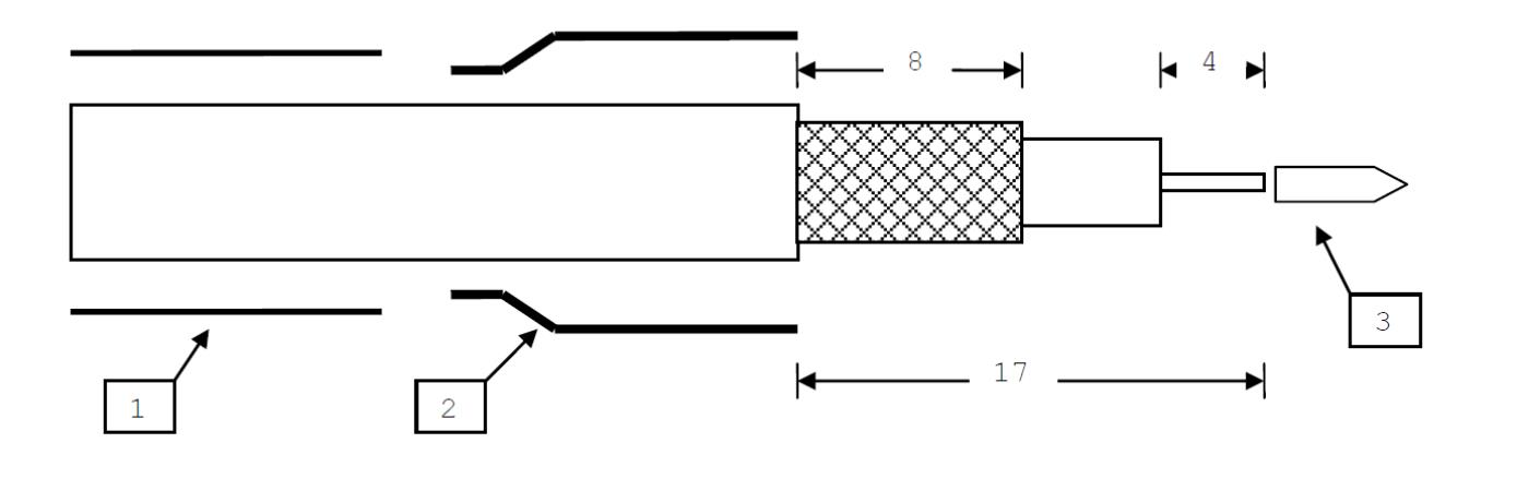
Assembly
- Slide a 25mm length of Heatshrink Sleeve [Item 1] EEl 16-04-01 over the cable
- Slide the ferrule [Item 2] over the cable as shown
- Trim back outer sheath, braid and dielectric as illustrated in the diagram
- Crimp the contact [Item 3] using the appropriate Crimp Tool
- Gently insert the crimped contact / cable sub assembly into the connector boady until fully located, at the same time ensuring that the cable entry part of the connector is inserted between the dielectric and the braid
- Slide the ferrule [Item 2] along the cable until it butts against the connector shoulder and crimp
- Slide the sleeve [Item 1] along the cable until it butts against the connector shoulder and shrink into place
Tool Return
Return the crimp tool(s) and dies to their appropriate storage area before leaving
Amendments to Procedure
Inform the Engineering & Technical Support Manager at the earliest opportunity if this procedure has, or needs to be altered in any wa
BNC Crimp Connector RG58: Assembly instructions
OH&S Requirements
- Ensure you have either completed a Risk Assessment or read (and confirmed as being read) the relevant Risk Assessment before attempting this task
- The UQ Risk Management Database is located at: www.risk.admin.uq.edu.au
Tool Options
This procedure has been written specifically for the following items:
- RG58 Crimp Connector: EEL 15-13-02
- RG58 Coaxial Cable: EEl 22-04-07
- Crimp Tool: K011 with die 2904 fitted
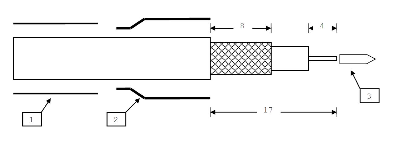
Assembly
- Slide a 25mm length of Heatshrink Sleeve [Item1] EEL 16-05-01 over the cable
- Slide the ferrule [Item 2] over the cable as shown
- Trim back outer sheath braid and dielectric as illustrated in the diagram
- Crimp the contact [Item 3] using the Crimp Tool K011
- Gently insert the crimped contact/cable sub assembly into the connector body until fully located, at the same time ensuring that the cable entry part of the connector is inserted between the dielectric and the braid
- Slide the ferrule [Item 2] along the cable until it butts against the connector shoulder and crimp
- Slide the sleeve [Item 1] along the cable until it butts against the connector shoulder and shrink into place
Tool Return
Return the crimp tool(s) and dies to their appropriate storage area before leaving
Amendments to Procedure
Inform the Engineering & Technical Support Manager at the earliest opportunity if this procedure has, or needs to be altered in any way
Chipbonder 3608: Application instructions
OH&S Requirements
- Ensure you have either completed a Risk Assessment or read (and confirmed as being read) the relevant Risk Assessment before attempting this procedure
- No Risk Assessment has be sighted as of 13/05/2012
- The UQ Risk Management Database is located at: www.risk.admin.uq.edu.au
- Visually check any equipment is safe to operate and the electrical safety tag is current. If expired, the equipment must be tested and tagged before proceeding
- Wear safety glasses, gloves and a lab coat before you begin
- Clean room protocols apply to the Darkroom / PCB Etching Facility
Application
- Apply Chipbonder EEL 97-10-02 using an appropriate needle
- Place drops in such a way that the adhesive is completely covered by the component
Curing
- Cure the assembly for 5 minutes at 150 deg C or 10 minutes at 130 deg C
- The product will not cure below 120 Deg C
- In cases where the adhesive drop is exposed e.g. S023 components, cure should be at 150 deg.
- Irradiation of assembly with UV light prior to curing will gel the exposed adhesive and allow to cure at 130 deg C
Additional Information
- The manufacturer's safety data sheet for Chipbonder 3608 EEL 97-10-02 is MSDS002
Amendments to Procedure
Inform the Engineering & Technical Support Manager at the earliest opportunity if this procedure has, or needs to be altered in any way
EEL CAD Libraries
The Electronics Engineering Laboratory Libraries have been created specifically to meet our PCB production requirements. Every effort has been made to ensure each library component is error free and fully compatible with current stock.
These files are for download only.
Create a new folder (e.g. <ETSG>) under the Altium Library folder
Extract required files into the new folder.
- Protel99 PCB Libraries (ZIP, 466.8 KB)
- Protel99 SCH Libraries (ZIP, 305.5 KB)
- Altium Designer 6 PCB Library KBpcb01 (ZIP, 62.5 KB)
- Altium Designer 6 PCB Library KBpcb02 (ZIP, 33.1 KB)
- Altium Designer 6 PCB Library KBpcb03 (ZIP, 19.5 KB)
- Altium Designer 6 PCB Library KBpcb04 (ZIP, 14.6 KB)
- Altium Designer 6 PCB Library KBpcb05 (ZIP, 28 KB)
- Altium Designer 6 PCB Library KBpcb06 (ZIP, 8.1 KB)
- Altium Designer 6 PCB Library KBpcb07 (ZIP, 3.4 KB)
- Altium Designer 6 SCH Library KBpcb01 (ZIP, 20.2 KB)
- Altium Designer 6 SCH Library KBpcb02 (ZIP, 1.2 KB)
OR - All above files as one zip file (ZIP, 0.9 MB)
EEL Data Sheet - PCB Design Requirements: External Manufacture (BEC)
|
Design Rules > Routing |
Protel 99 Path = Design > Rules > Routing |
|
|
> Clearance Constraint |
= 10mil : Preferred (All Objects) |
|
|
> Routing Via Style |
= 50mil dia / 20mil hole : Preferred Size = 30mil dia / 20mil hole : Minimum Size |
|
|
> Width Constraint |
= minimum 10mil = preferred 12mil = maximum user defined |
NB: Wider tracks are mechanically superior. Choose carefully! |
|
Design Rules > Manufacturing |
Protel 99 Path = Design > Rules > Manufacturing |
||
|
> Hole Size Constraint |
= minimum 12mil : Define hole sizes in 4mil increments = maximum user defined : starting at 12mil (0.3mm) |
||
|
> Minimum Annular Ring |
= minimum 10mil EXTREMELY IMPORTANT! |
||
|
> Polygon Connect Style |
= Rule Attributes = Conductor Width = Conductors = Angle = Filter Kind = Pwr Plane Clearance |
Relief Connect 15mil 4 90 Angle Whole Board 20mil |
: Nominal : Nominal : Nominal : Nominal : Nominal : Nominal |
|
Design Options > Options |
Protel 99 Path = Design > Options > Options |
||
|
> Grids |
= Snap X = Snap Y = Component X = Component Y |
25mil 25mil 25mil 25mil |
: Nominal : Nominal : Nominal : Nominal |
|
> Measurement Unit |
= Imperial |
Inches |
: Preferred |
Position in Workspace
Place the PCB design such that the lower left corner of the PCB is at workspace coordinate 1000mil, 1000mil.
Borders
- Ensure the PCB border is created on Mechanical Layer 1 using 10mil tracks
- It is recommended that there is a minimum clearance of 120mil (3mm) between the border and all PCB elements
Identification
All printed circuit boards shall be idented on an appropriate layer (Nominally, Top Overlay). Please note: boards presented for manufacture wihout a suitable ident will be rejected.
Mounting Requirements
- Do you need mounting holes
- For M3 mounting holes use PCB library component SPACER01 in KBpcb05 library
Final Checks
- Ensure you check your schematic running ERC, and PCB by running DRC
- Further information regarding PCB design requirements may be found at www.becman.com
Libraries
It is important to note that a large number of PCB footprints intended for through hole components supplied by Protel are incompatible with our manufacturing process.
It is therefore recommended that you use the Electronics Engineering Laboratory Libraries which support many of the components held by this facility and are fully compatible with our PCB manufacturing process.
Schematic and PCB libraries are available for download from the Engineering & Technical Support Group website.
If you have already designed your PCB using (TH) footprints supplied by Protel, it is suggested that you carry out a thorough inspection with respect to physical size, annular ring and hole size requirements for each component before submitting your design for manufacture.
Library Catalogue Access
The Protel Library Catalogue displays the contents of our Schematic and PCB Libraries and is accessible at the following locations:
- Electronics Engineering Lab student computing area > Non-removable hard copy
- Engineering & Technical Support Group website > PDF files for download
Feedback
Please email any suggestions to the Engineering & Technical Support Group Manager
Electronics Engineering Laboratory Data Sheets
EEL Data Sheets explained
The primary purpose of an EEL Data Sheet is:
- To provide general or engineering information relevant to the day-to-day operations of the Electronics Engineering Laboratory
- To provide a medium by which information is permanently retained for future reference
Please note - EEL Data Sheets are for information only and do not necessarily constitute part of a formal process or procedure.
Register of EEL Data Sheets
Current:
- Component Data Sheets:
- Data Sheets 0001 - 0250
- Data Sheets 0251 - 0499
- Data Sheets 0500 - 0501
- International Protection (IP) Codes (below)
- Transistor Footprints
- Multi Layer PCB Assy - 4 Layer
- Multi Layer PCB Assy - 6 Layer
- Multi Layer PCB Assy - 2 Layer
- Metric to Imperial Conversion Table
- PCB Specs - 97-04-01
- ETSG SMD pcb adaptor files (Altium)
Require Updating:
- PCB Design Requirements - Etched
- PCB Design Requirements - Milled
- PCB Design Requirements - BEC
No Longer in Use
- NC Drill K076 Tool Codes
- Anechoic Chamber Power Up Information
EEL Data Sheet - International Protection (IP) Codes
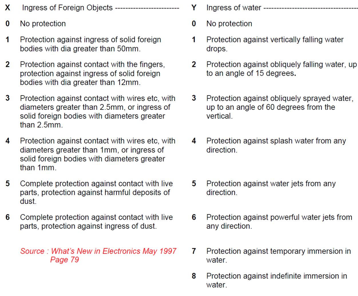
Code Format
IP = International Protection
X = 1st Numberal - Ingress of foreign objects
Y = 2nd Numberal - Ingress of water
Code Definitions
Amendments to Data Sheet
Inform the Engineering & Technical Support Group Manager at the earliest opportunity if this information needs to be altered in any way
EEL Data Sheet - Transistor Footprints
Transistor Footprints - EEL Protel Libraries
EEL Protel 98 Transistor Footprints:
BC179 T018
BC547 TO92/B
BC548 TO92/B
BC549 TO92/B
BC557 TO92/B
BC558 TO92/B
BC559 TO92/B
BD139 TO126/*
BD140 TO126/*
BD649 TO220/*
BDT63C TO220/A
BF470 TO126/*
BF469 TO126/*
BUK456 TO220/*B
BUK553 TO220/*B
IRF9520 TO220/*B
MJ15003 TO3/*A
MPSA42 TO92/C
MPSA14 T092/C
PN3640 TO92/C
PN4356 TO92/C
VN10LM TO92/G
2N2222 TO18
2N3019 TO39
2N3638 TO18
2N3639 TO18
2N3644 TO92/C
2N3700 TO18
2N3702 TO92/A
2N3703 TO92/A
2N3704 TO92/A
2N3705 TO92/A
2N3903 TO92/C
2N3904 TO92/C
2N3905 TO92/C
2N3906 TO92/C
2N4033 TO39
2N4393 TO18/A
2N5087 TO92/C
2N5400 TO92/C
2N5485 TO92/F
2N5700 TO92/C
2N6123 TO220/*A
2N7000 TO92/G
2SJ49 TO3/1B
2SK134 TO3/1B
ZTX651 E-LINE/B
ZTX658 E-LINE/B
ZTX751 E-LINE/B
Amendments to Data Sheet
Inform the Engineering & Technical Support Group Manager at the earliest opportunity if this information needs to be altered in any way.
N Type Crimp Connector RG58: Assembly Instructions
OH&S Requirements
- Ensure you have either completed a Risk Assessment or read (and confirmed as being read) the relevant Risk Assessment before attempting the task
- The UQ Risk Management Database is located at: www.risk.admin.uq.edu.au
Tool
This procedure has been written specifically for the following item:
- RG 58 Erma Crimp Tool: K011 with Die 29204 fitted
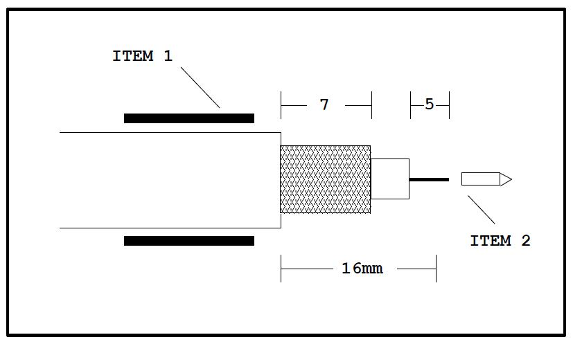
Assembly
- Place sleeve [Item1] over cable
- Trim back outer sheath, braid and dielectric to indicated dimensions
- Crimp the centre pin [Item 2] using the RG58 Erma Crimp Tool
- Press sub assembly into body ensuring the ferrule is inserted between the dielectric and the braid
- Slide sleeve [Item 1] along cable until it butts against the ferrule shoulder, then crimp using the RG58 Erma Crimp Tool
Tool Return
Return the crimp tool and die to the appropriate storage area before leaving
Amendments to Procedure
Inform the Engineering & Technical Support Manager at the earliest opportunity if this procedure has, or needs to be altered in any way